
Nanoelectronics in which the semiconductors main characteristics include memory logic transistors and other parts are measured at less than 100 nanometers is growing rapidly. Potential applications for quantum computing advanced memory and even the storage and generation of energy are tiny devices with enormous potential.
History of Nanoelectronics
One of the first electronics to be nanoscale were developed by researchers in the 1960s. They developed gold thin films that were only 10 nanometers thick to be used as the base of junction transistor.
In the early 1980s in the 1980s team of IBM researchers created the worlds first field effect transistor (MOSFET) that had its gate oxides thickness at 10 nm. The transistor was created with the tungsten gate method to achieve this nanoscale dimension.
The first three gate MOSFET which was one of the first multi gate MOSFET named the FinFET was developed in the year 1989. The FinFET also referred to as the Fin field effect transistor was double gate MOSFET that is tridimensional and non planar. In 2002 10 millimeter FinFET was produced.
A CMOS (complementary MOS) transistor was developed in 1999 in order to illustrate how MOSFET transistors could do to help us in the direction towards the development of Nanoscale electronic gadgets.
In 2006 researchers come up with the MOSFET which had dimension of less than 3 nm which made the tinyst ever device of the moment.
Nanoelectronic semiconductors were first commercially produced in 2010s decade. In the following year Samsung is presently releasing the nanometer sized GAAFET that is gate all round FET that can be purchased.
How Was Nanoelectronics Made Possible?
Nanoscale electronic devices are the culmination of the latest products of years of top of the line research into nanosciences as well as nanotechnology.
The idea of Richard Feynmans possibility of computers using “submicroscopic” computers in amazing lecture in 1959 researchers in the very forefront of instruments physics engineering and materials science as well as the research into manufacturing are conducting ever test sizes.
This led to variety of revolutionary technologies that use the technology of information and communication (ICT) like personal computers phones Internet of Things (IoT) technology and much numerous others. Everyday game changers of the future are due to the latest advances in Nanoelectronic research.
The nano electronic gadgets have not yet hit the shelves in our shops.
The development of semiconductor technology has been significant but microcomputers remain very far off. Sub micron (nanoscale) computers may still be quite ways off.
The semiconductor technology may be limited in terms of the size of the system. We may have reached that point.
Nanoelectronics which is currently in study could help us overcome this obstacle through the production and development of sub micron nano scale electronic devices in the next couple of years.
Moving Nanoelectronics Forward
Researchers have suggested the best method for creating nanoelectronics is to combine electronic devices made of microelectronics with nanoelectronics to create hybrid devices.
This approach builds on the progress already achieved in microelectronics for example in developing microelectromechanical systems (MEMS) technology which has brought numerous MEMS sensors like accelerometers and microphones magnetometers and gyroscopes and even power generators to the market.
One of the most innovative developments using the hybrid approach is the quantum effect nanoelectronic device which is employed for resonance tunneling. The device uses standard Silicon bulk effect transistor to make multi state switching device which its inventors describe as”a “resonance tunneling transistor.”
The resonance tunneling transistor can be utilized to construct circuits with higher quantity of available logic that the standard microelectronic transistor could provide.
Another device in investigation could be the single electron transistor also known as the SET. Its switch device that controls electron tunneling using this method to increase the strength of current.
Two tunnel junctions made up of two parts made of metal that have very thin and sub nanometer thick layer of insulation in between possess identical electrodes. Electrons must travel through the insulator to move between the electrodes.
Because quantum tunneling is an independent process which generates electric charges electrons moving over the tunnel junction. Electric charges are produced in huge quantities of each electrons charge.
Electronic tunneling devices as well as quantum dots work with quantum energy. Quantized energy is composed of the smallest number of parts that can interact. It is at the level of quantum physics phenomena like tunneling particle entanglement and superposition. particles. They are also evident.
Nanoelectronics technology can release electrons within extremely tiny regions. Naturally the measurement of energy as well as the impact it exerts on the devices as well as the functions they are able to serve are important fields of research in the near future.
Another area of interest within the realm of nanoelectronics is the exploration of ways to use electroconductive polymers in tiny scale electronic circuits made of organic material.
Researchers are examining electricallyconductive nanostructured polymers and nanoparticle based ones as well as polymer nanocomposites containing Nanoparticles that conduct electricity.
Theyre perfect for the creation of nanoscale electronic devices which are composed of organic. This is due to capabilities of nanopolymers to function as building blocks which can be used to create simple or more complex nanostructures.
Organic and nanostructured nanoelectronics devices are capable of being used with polymers that have been conjugated to electron acceptors for the new Generation of organic photovoltaics on nanoscales.
Spintronics
In addition to transistors the nanoelectronic devices also play role with the data storage information (memory). This is why spintronics the study and development of electron spin as well as the magnetic moment associated with charge electrical is an old technology. Read more: ” Graphene spintronics from science to technology”.
Additionally it will have role to contribute to the development of technology which harnesses quantum properties to calculate (read more about it in ” Quantum computing moves forward with spintronics progress” and ” The birth of topological spintronics”).
Optoelectronics
Electronic devices which produce light regulate it and identify it as well as regulate lighting i.e. optoelectronics come in variety of forms and styles. Theyre very energy efficient (less energy and heating) optical communications are becoming ever more significant due to the potential to solve one of the greatest challenges we confront in todays information age the energy issue.
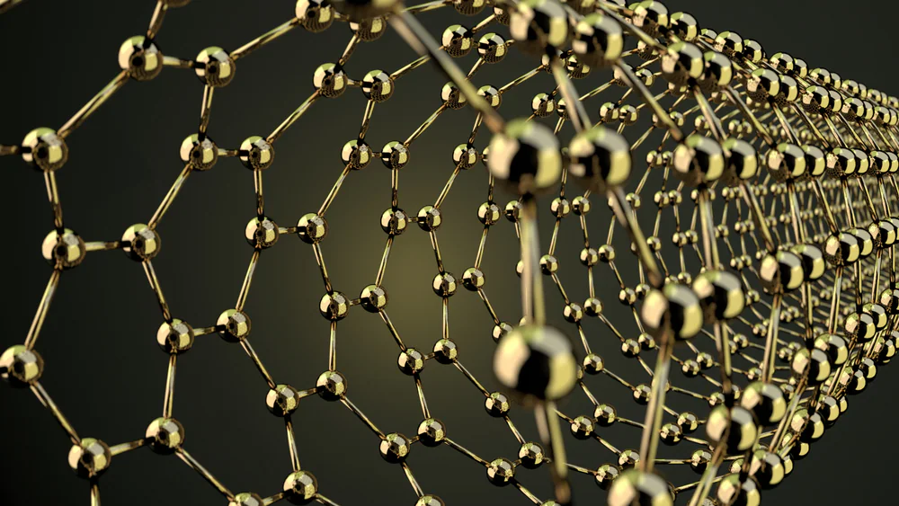
Nanotechnology is field of study. Nanoparticles like nanoparticles (see the following example: ” Light emitting nanofibers shine the way for optoelectronic textiles”) along with carbon nanotubes are being utilized specifically graphene. It has shown incredible potential for optoelectronic circuits.
Displays
Display technologies are classified in three broad areas of technological innovation: Organic LEDs Electronic printing and other technology that displays images in stills and field emission Displays. For further information go to our post on Nanotechnology to display.
Wearable flexible electronics
The age for wearable devices on the market is here as demonstrated by the rapid development of fitness band devices and other next generation tools for tracking your health such as electronic tattoos.
Research findings provide proof of wearable electronics in the making and will go beyond small electronic devices which are also termed wearable computers. The devices wont just be integrated into textiles however the electronic gadget or system could evolve into cloth. Electronic fabrics (e textiles) can enable the development and manufacture of new types of clothes that have electronically controlled sensors that are distributed across the entire garment. These types of fabrics are likely to become revolutionary in their capacity to sense the surroundings and perform and emit signals such as biomedical monitors or advancement of man machine interfaces and in the best situation utilize the current textile manufacturing system which is cost effective (see examples such as ” wearing single walled carbon nanotube electronics on your skin” and”abstract tattoos that monitor blood sugar levels” ” temporary tattoo to monitor glucose levels” or ” graphene nanosensor tattoo on teeth monitors bacteria in your mouth”).
Nanoelectronics in Energy
Solar cells and supercapacitors are just two of the fields that nanoelectronics performs major role in the generation of energy as well as in storage. For more details refer to the articles weve published on Nanotechnology in Energy and Graphene Nanotechnology for Energy.
Molecular Electronics
As opposed with nanoelectronics that can be scaled down to nanoscales molecular electronic devices are concerned with the electronic functions which are located in molecular structures similar to those that are discovered in nature. These include the process of photosynthesis as well as signal transduction.
The purpose for Molecular Electronics is to develop the basic knowledge of the process of charging molecules. This is driven by the need to develop molecular circuits to enable to create tiny high performance and energy efficient computer systems (see examples: ” Adding an optoelectronic component to molecular electronics”).
Electronic materials are utilized to develop applications.
Nanoparticles can be used as dielectric substances conductive materials as well as piezoelectric materials because they are easy to charge electrons and later let them go. The field of nanoscience and technology of nanoelectronics and technology is the base of the area that is nanoscience technology and. Nanoelectronics and Science is natural extension of advances in microelectronics. It is however innovative field in which its possible to construct quantum structures quantum devices and quantum circuits and quantum systems based on the concepts of fresh ideas.
Nanoelectronics could break through the limits of traditional technology making use of the structure as well as data capabilities of the materials. They can significantly increasing the capacity to process and store information per unit of material. They can also make revolutionary advancements in the gathering of data and processing capabilities.
Because of the vitality of nanoelectronics in the world of technology for information United States the European Union Germany and Japan are currently putting together strategy to develop that incorporates Nano Electronics Technology and deployed initiatives. The end of the 20th century research in the nanoelectronics area was being developed in China along with Japan. Nanoelectronics is now acknowledged as the principal field of development and research in the area of nanoscience and technology over period of time.
Affected by the policies of various nations nanoelectronics has grown rapid throughout the world over the last decade. Recently silylene and black phosphorus hexagonal boron Nitride transition metal salts and monolayer molybdenum disulfide are one of the most prominent developments in the field of study of materials in nanoelectronics. Additionally in contrast to oxides metals and crystals the research into semiconductors is also growing dramatically.
Gallium arsenide as well as silicon are two kinds of semiconductors that require more research. Research on gallium arsenide continues to expand whereas investigation into silicon has decreased however the precise proportional reduction is not clear. The research on graphene along with boron Nitride and molybdenum disulfide are increased. When compared with carbon nanotubes and silicon nanowires and other nanowires that have decline in research papers graphene nanobelts and epitaxial graphene have higher growth in research papers.
Nanomaterials are extensively used and are becoming more advanced technology in electronics. Zhang et al . [66] proposed different approaches to prepare flexible electronic devices constructed on LM nanoink. This is an extensive field of use that can be used to create printed electronic devices. The LM nanoink is device that regulates biocompatibility and stability and could be an essential component for the future design of devices that incorporate flexibility in electronics.
Nanopowders and particles are widely utilized in nanoelectronics technology and science which includes electronic devices made of nanoparticles that work with microelectronics have become hot topic. Since the beginning of the 20th century the technology that was that was based on nanoelectronics has had huge impact on our lives as well as the work we do.
As per Moore law volume of the integrated circuits (IC) has been increasing at rate of 4 times that per 3 years. These dimensions have decreased over the last 30 years. The dimensions of electronic gadgets has been decreasing as well as the requirements for the Integration of integrated circuits is becoming more complex. Finding methods to make more affordable and efficient semiconductor chips is an essential matter that must be understood by everyone.
For making smaller electronic devices they are more durable. it is currently the trend to integrate nanotechnology into electronic devices. Nanoscale electronic devices could be further reduced since the performance of such devices is closely be correlated to the quantum properties of the device.
The addition of graphene nanoparticles into the cooling process as in the cooling process Babith Lawrance as well as Renish have dramatically enhanced the efficiency in convective transfer of heat water. This has substantial cooling effect when compared with conventional cooling methods [67]. Quantum nanoelectronics are able with the ability to accomplish greater tasks in relation to changing the frequency of electron wave. They also have higher efficiency and less consuming so that they can solve the problem of using energy.
Optoelectronics today has slowly advanced to the latest nanooptoelectronic technology and development of nanooptoelectronics was integrated into the development of standard semiconductors. It eventually it has been recognized as groundbreaking technology which will become an important step forward in the development of nanoelectronics which are gaining momentum.
Nanotechnology can help us understand the connection between photons and electrons within every nanostructure. The end result is that photoelectrons as well as nanoelectronics technology merge. The new research and technology Nanooptoelectronics the result of the convergence of both science and engineering and also the outcome of continuous advancements of technology being used.
The same is true for nanotechnology. an outcome of the mix of nanotechnology and electronics nanooptoelectronic technology will allow people to manipulate single atom according to their wishes. Nanooptoelectronics are typically electronic components in addition to nanoelectronics.
Nanoelectronic devices include nanophotoelectric devices nanoluminescent display units nanodisplays and many more. The detectors of nanophotoelectric technology are usually made up of nanowires and variety of nanorods or nanopowders which are coated. Infrared detectors are the most sought after devices made of nanophotoelectric technology. It extremely sensitive when utilized.
The advent of nanooptoelectronics as well as other elements that are essential modern light emitting nanomaterials are being built. From structural perspective from structural standpoint one could think of making an use of different kinds of nanoparticles as an illuminated silicon diode. We can then utilize wide range of sizes for wide variety of diodes emitting luminescence. In addition the research area of nanodisplay has become technologically modern.
Most commonly used display made of nanotubes is composed of large portion of nanotube displays as well as display panels made of carbon. This technology is able to increase the performance of computer on computer. It may even slow down the rate of computation within an extremely short time.
The capacity of computers used is fraction of that of the computers currently on the market. Nanooptoelectronics can often increase the capability of communication by hundreds of times.
Nanoelectronics technology is an technology with lot of potential as well as an enormous range of applications. Nanoelectronic technology is developing
by combining nanotechnology and the latest electronic components they is able to increase the market. The technology also creates more specifications to create electronic components which are in the process of becoming and are gradually moving forward in the development process to turn the components into useful items.
The advancement of single electron devices nanofield effect transistors molecular electronic devices as well as other ingenious technology are continually evolving due to the research conducted.
Conclusions
The sector of nanoelectronics is growing rapidly which involves the development of nanosensors in nano sized size to be used “from home to field.” Nanoelectronic devices will be essential in the advancement of analysis of high performance. Researchers are currently developing sensors that could be used to perform “bed side analyses” and “point of care.”
The sensor that is portable is considered as good one when its easy to use that displays information live and in real time and also is able to determine precisely. There are few nano sized devices that exist commercially are the result of nanoelectronics. In the future advances in nanoelectronics may lead to variety different sensors suitable for range of purposes.